
VIP member

Product details
Brief introduction
Lumina AT1Optical surface defect analyzer can be used forGlassSurface testing of semiconductor and optoelectronic materials.Lumina AT1Can detect bothSiC、GaNTransparent materials such as sapphire and glass can alsoSiTesting is carried out on opaque substrates such as gallium arsenide and indium phosphide,Its price advantage makes itbecomeSuitable for research and development/Small batch production processA powerful tool for quality management and yield improvement.
Lumina AT1Combining scattering measurement, elliptical polarization, reflection measurement, andSurface slopeBased on the fundamental principles, non destructively analyzeWaferDetect residual foreign objects on the surface, surface and subsurface defects, shape changes, and uniformity of film thickness.
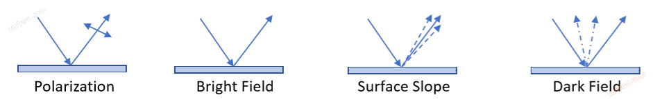
1.Polarization channels are used for thin films, scratches, and stress points;
2.Slope channels are used for pits and protrusions;
3.Reflective channels are used for particles on rough surfaces;
4.Dark field channels are used for particles and scratches;
II function
lmajor function
1. Defect detection and classification
2. Defect analysis
3. filmuniformitymeasure
4. surface roughness measurement
5. Thin film stress detection
lFEATURES
1.Transparent, semi transparent, and opaque materials can be measured, such as silicon, compound semiconductors, or metal substrates;
2.Realize full surface scanning and imaging of sub nanometer thin film coatings, nanoparticles, scratches, pits, protrusions, stress points, and other defects;
3.150mmThe scanning time for full surface scanning of wafers is3minute,50x50mmsample30Scan and display results within seconds;
4.High seismic performance, non rotating system, shape independent, capable of accommodating non-circular and fragile base materials;
5.up to300x300mmThe scanning area; Defects can be located for further analysis; Technical capabilities
3、 Application Cases
1. transparent/Non transparent material surface defect detection

2. MOCVDDefect control of epitaxial growth film formation
3. PREvaluation of film thickness uniformity
4. CleanEvaluation of Process Cleaning Effectiveness
5. WaferexistCMPAnalysis of Rear Surface Defects
6. Multiple application areas, such asAR/VR、Glass, photomask template, sapphireSiwaferclass

Online inquiry
-
Contacts
-
Company
-
Telephone
-
Email
-
WeChat
-
Verification Code
-
Message Content
-